Measuring neutrons produced by nuclear reactions, whether fission or fusion, is a major challenge for performance evaluation and safety. A team involving the four operational divisions of the CEA has developed an innovative neutron detector by encapsulating a SiC diode in a robust assembly. This work, which has just been patented, paves the way for a new generation of compact, robust detectors suitable for extreme environments such as those of the Jules Horowitz reactor, ITER, and the Laser MégaJoule.
Neutron sensors are generally integrated into particularly challenging measurement environments: high levels of radiation, operating temperatures, electromagnetic fields, and reduced accessibility limiting or even preventing maintenance operations. Conventional detection assemblies, consisting of a sensor assembled in a mechanical mounting with signal transfer, may have a limited service life.
In this hostile measurement environment, silicon carbide (SiC) has emerged as a promising material for producing a signal following interaction with a neutron. This wide bandgap semiconductor has thermomechanical properties that enable the production of sensors capable of providing stable measurements at high temperatures. The study of SiC was first the subject of a thesis between DRF/IRFM, DES/IRESNE, and Aix-Marseille University, focusing on its intrinsic behavior under hostile conditions. A second project, supported by the CEA’s Transverse Skills Program (PTC) for instrumentation, then aimed to design a complete neutron detector by encapsulating a SiC diode in a robust assembly.
This project involved numerous teams from the CEA: DRT/CEATech Occitanie (ceramics), DES-Gre/LITEN/DTNM and DEHT (metals, screen printing, electrical characterization), DRT-Gre/LETI/DOPT, DPFT, and DCOS (characterization, machining, cutting, and diode integration), DES-Sac/ISAS (concept and process selection), DRF-Cad/IRFM and DES-Cad/IRESNE (testing on the WEST tokamak and under neutron flux), CEA-DIF/DAM/DCRE (applications at LMJ).
The originality of the project lies in the combination of two innovative processes:
- additive manufacturing, used to produce complex parts in alumina and CuCrZr alloy;
- Spark Plasma Sintering (SPS), a current-assisted sintering process that enables rapid and efficient sealing, ensuring both the mechanical integrity and electrical continuity of the assemblies.
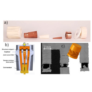
The final design took the form of a coaxial assembly of seven parts: copper electrodes with controlled deformation zones, an alumina outer casing, and joints sealed with borosilicate glass frits applied by screen printing (Figure 1).
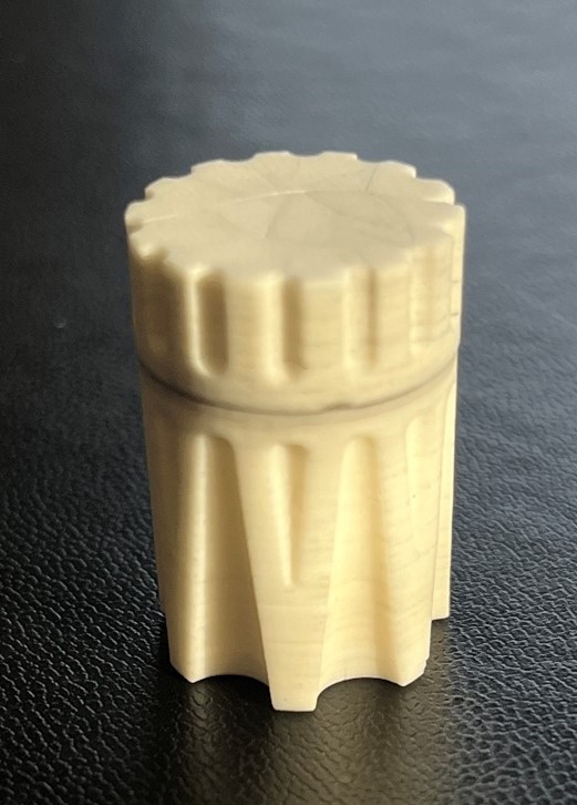
Figure 1: Prototype encapsulation of a SiC neutron sensor using additive manufacturing. Diameter 15 mm x height 25 mm.
Thermo-electro-mechanical simulations guided the optimization of geometries, for example by integrating origami structures into the electrodes to improve contact with the diode or by refining the alumina walls (< 4 mm) to limit cracking at high temperatures (Figure 2).
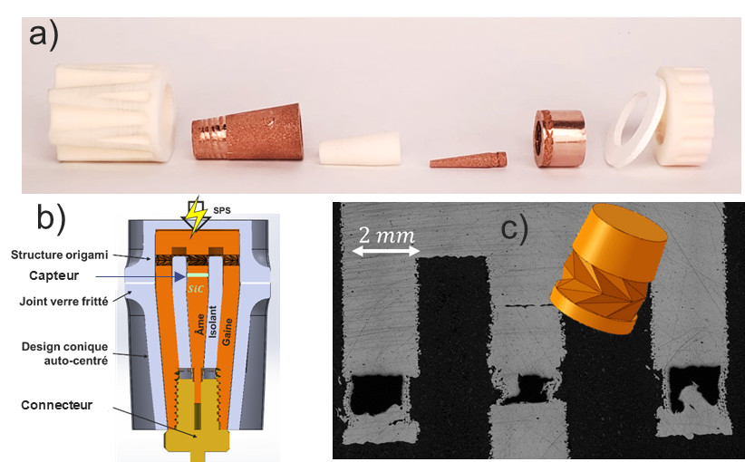
c) X-ray showing the deformation of the origami areas after sealing by SPS.
Optimization work has led to the development of an ultra-fast SPS cycle, reducing material diffusion around the sensor, significantly reducing leakage currents compared to a slow cycle, and thus preserving the integrity of the SiC sensor. Characterization of the detector showed no degradation in performance due to the SPS process and the various stages of additive manufacturing. A final test on a 14 MeV neutron generator confirmed the ability of the complete device to perform neutron measurements: the measured pulses (lasting a few nanoseconds and with amplitudes of a few mV) show the characteristic signature of neutrons in this type of sensor.
This work has been patented [1] and is currently being published [2]. This first prototype is the first demonstration of a thin semiconductor-type fast neutron detector encapsulated in an assembly manufactured using additive manufacturing and sealed by SPS. This work paves the way for a new generation of compact, robust detectors suitable for the extreme environments of facilities such as the Jules Horowitz Reactor, the ITER tokamak, and the MegaJoule Laser.
[1] Brevet DRF : « Encapsulation_diode_SPS », BD25291 AL.
[2] L. Ravix et al., « Conception of a semi-conductor neutron detector with additive manufactured parts and Field Assisted Sintering Technology packaging”, Revue of Scientific Instruments